D.I.Y. Patch Antenna

Category: AcubeSAT

D.I.Y. Patch Antenna

In order to successfully complete our mission, it is necessary to downlink images ⁠—taken during our experiment⁠— from AcubeSAT to our Ground Station. To achieve this, we use an in-house patch antenna, which operates in the frequency of 2.4GHz.

You can read more about patch antennas here:

Let’s now create together the antenna for our mission!

Supplies you will need:

Extra consumables:

Let's get to the good part

Step 1

Print at least 3 copies of the metal patch on a transparent film using black jet. Stack them together, making the desired area opaque, in this way creating a photomask.

The design of the metal patch can be found here.

Step 2

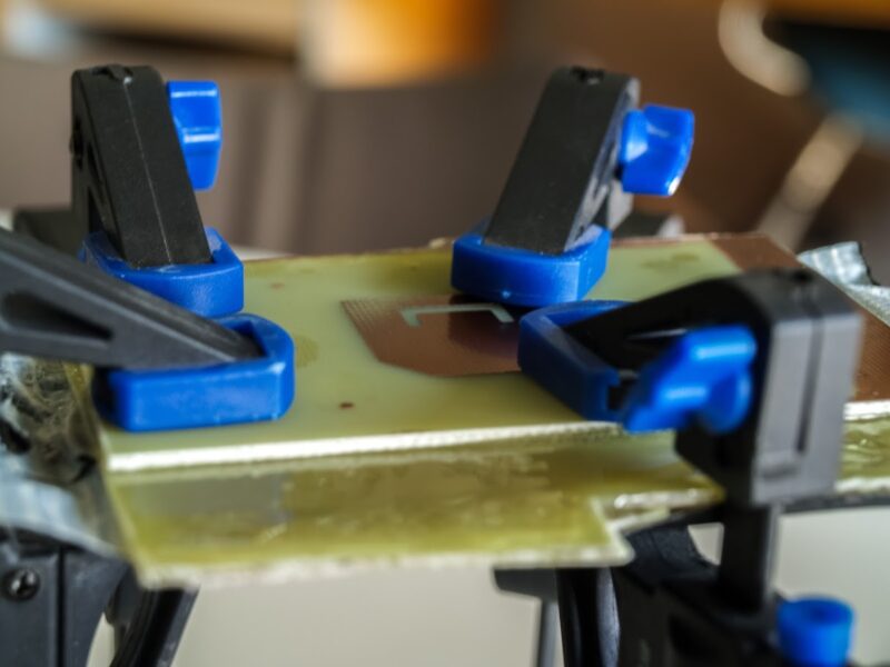
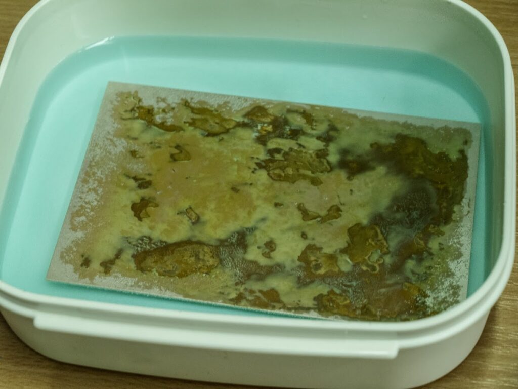
Remove the protective cover from the photosensitive PCB. 

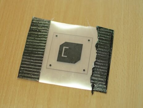
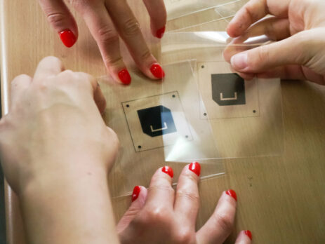
Apply the previously created photomask on top of the photosensitive and put a glass on top of it. 

Leave the layer exposed in the sunlight for about 4 minutes.

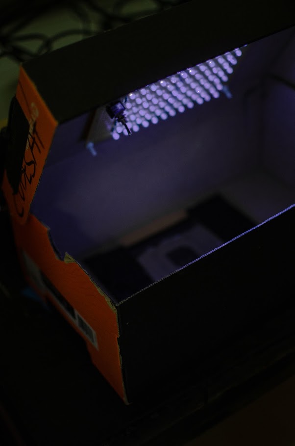
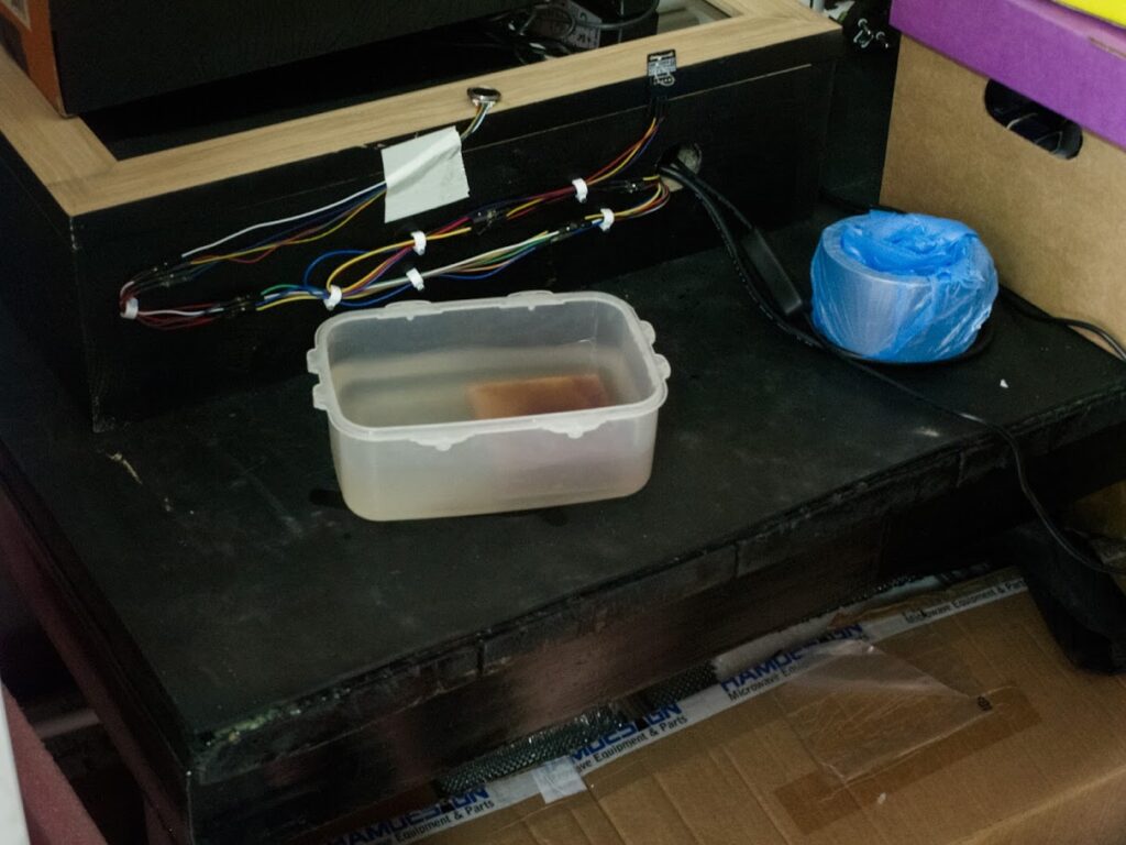
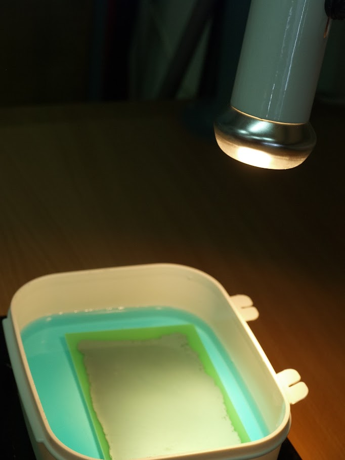
As an alternative, you could expose the layer in UV Light with the help of a DIY UV Led Exposure Box for about 10 minutes.
You can find instructions for a DIY UV Led Exposure Box here.

Step 3

Create a DP50 developer solution following the instructions in the developer’s packaging.

Submerge the photosensitive in the solution for 30 seconds.

Important note: Τhe area that was exposed to UV light is soluble on the developer solution, allowing to etch the copper only in desired areas.

Tip #1: If the whole copper layer is removed in the developer, in your next try, let the photosensitive exposed to the sunlight a little bit longer.

Step 4

Sand the inner sides of the PCBs with P80 and then P120 sandpaper.

Step 5

Apply epoxy glue on the inner sides of the PCBs, bond them and hold them together using clamps.

Tip #2: Use a vacuum desiccator if available and let the bonded PCB inside, in order to remove any bubbles formed between the layers, which will change the dielectric constant of the PCB.

Optional Step

In case you cannot find a FR4 PCB, you can always create one, by removing the copper layer of a basic PCB. 

What you will need:

Dissolve the Sodium Persulfate B327 into tap water following the instruction on the packaging.
Then dip the PCB inside, until its copper layer is removed.

Tip #3: Try to smoothly use a brush to remove any remaining copper from the top of the board.


Tip #4: Use the thermometer to control the solution’s temperature. It is important to keep its temperature at about 50 Celcious degrees. To achieve this, you may use a thermal lamp.

Did you enjoy this procedure? Do you want to create more antennas and learn about the communication processes between AcubeSAT and the Ground Station?


If yes, check the open positions on our website and apply for the COMMS Subsystem!

Share this post